 English
If you need the direct engineering answer before wading through pages of technical documentation: an LED display board works through a synchronized chain of digital video processing, high-speed serialization, FPGA spatial decoding, and constant-current multiplexed switching. A video source feeds raster frames into a sending processor, which packages pixel data into Gigabit Ethernet streams; receiving cards inside the display cabinet de-serialize this data and generate high-frequency Pulse Width Modulation (PWM) signals along with row-scanning address pulses across HUB75 interfaces; finally, specialized driver ICs sink precise constant currents through surface-mounted red, green, and blue light-emitting diodes, pulsing them thousands of times per second so human vision perceives a seamless, full-color dynamic image.
When evaluating led display board working principle manufacturers, buyers and system integrators frequently get lost in marketing buzzwords like "ultra-black surface" or "golden viewing ratio." But when you pull a magnetic module off its die-cast chassis and look at the bare printed circuit board under a magnifying lamp, what is actually happening? Why does a display with the exact same pixel pitch look buttery smooth and color-accurate from one factory, while another unit from a budget assembler flickers on camera and develops dark horizontal lines after six months of operation?
To make informed hardware decisions, you have to understand the fundamental physics, electrical engineering, and manufacturing trade-offs happening behind every square inch of silicon. Let's trace the complete journey of a video signal from the graphics processor down to individual photon emission, breaking down how tier-1 factories engineer these systems to operate reliably for years.
A large-format LED display is not a single monitor. It is a distributed network of thousands of tiny slave computers working in microsecond synchronization. To see how they cooperate, we can trace the signal pipeline through its five fundamental stages.
[Media Server / PC Video Out (HDMI / DP)]
                    │
                    ▼
[Video Processor / Sender]  ──> Color Management, Scaling, EDID, Frame Buffering
                    │
                    ▼  (Gigabit Ethernet Cable - Cat6, UDP / Custom Protocol)
[Cabinet Receiving Card (FPGA)] ──> De-packetization, Gamma LUT, PWM Generation
                    │
                    ▼  (16-Pin HUB75 / HUB75E Flat Ribbon Cable)
[LED Display Module PCB]
    ├──> Shift Registers & Driver ICs  ──> Constant-Current Column Sinks
    └──> P-Channel Line MOSFETs        ──> High-Side Row Scanning Decoders
                    │
                    ▼
[SMD / GOB / COB LED Diodes]           ──> Additive Photon Emission (RGB Mixing)
The process begins at your media player, broadcast switcher, or graphics workstation, outputting uncompressed digital video over HDMI, DisplayPort, or 12G-SDI.
Resolution Scaling & EDID Management: Standard video feeds arrive in conventional display resolutions (like 1920×1080 or 3840×2160). However, custom LED video walls almost never conform to standard aspect ratios. A building facade might measure 2400×600 pixels. The video processor crops, scales, and aligns the source canvas to match this non-standard layout.
Frame Rate Conversion & Genlock: For broadcast studios and virtual production stages, the processor locks its internal clock to an external bi-level or tri-level sync signal (Genlock). This ensures the LED refresh cycle matches the camera shutter angle down to the microsecond, eliminating rolling shutter tearing.
The processor's internal sending engine slices the master image canvas into discrete rectangular regions assigned to specific physical output ports.
A standard 1Gbps Ethernet port delivers an effective video payload capacity of roughly 650,000 pixels at 60Hz 8-bit color depth (or ~520,000 pixels at 10-bit).
Rather than sending standard TCP/IP packets with heavy protocol overhead, manufacturers use stripped-down, proprietary Layer-2 broadcast protocols running over UDP. Pixel coordinates and grayscale values are serialized into continuous high-speed data bursts traveling down standard Cat5e or Cat6 twisted-pair cables.
Inside each individual cabinet sits a receiving card (commonly built on Xilinx, Intel Cyclone, or Gowin FPGAs). This card serves as the local processing brain for that specific cluster of modules.
De-serialization & Spatial Mapping: The FPGA captures the incoming Ethernet stream, strips away transmission headers, and buffers the frame data inside onboard high-speed SDRAM or DDR memory.
Gamma Correction & Color Calibration: Raw digital video uses a gamma curve optimized for standard monitors. The FPGA applies a 16-bit to 18-bit lookup table (LUT) to expand low-grayscale detail and applies factory-calibrated chromatic coefficients. This calibration ensures that every individual module produces identical color temperatures and luminance steps.
HUB75 Stream Generation: The FPGA splits the buffered frame into parallel data channels and clocks them out through multi-pin headers to the physical display modules.
At the physical core of the display board are light-emitting diodes. An LED is a compound semiconductor p-n junction diode that converts electrical current directly into light through a quantum phenomenon known as electroluminescence.
When forward-bias voltage is applied across the p-n junction:
Electrons from the n-type conduction band cross the junction and recombine with electron holes in the p-type valence band.
As these charge carriers fall into lower energy states, they release energy in the form of discrete photons.
The precise wavelength (color) of the emitted photon is dictated by the bandgap energy of the semiconductor substrate material.
Direct Bandgap Semiconductor Materials:
• Red Diodes:    AlInGaP (Aluminum Indium Gallium Phosphide)  ──> ~620nm - 630nm
• Green Diodes:  InGaN   (Indium Gallium Nitride)            ──> ~520nm - 530nm
• Blue Diodes:   InGaN   (Indium Gallium Nitride)            ──> ~465nm - 475nm
Because human eyes possess three types of color-sensing cone cells (sensitive to long, medium, and short wavelengths), we can generate virtually the entire visible color gamut by adjusting the relative luminous intensity of these three primary emitters placed tightly side by side. This additive color synthesis happens in real time across millions of sub-pixel triads.
A common question among engineers new to display hardware is: why not simply vary the forward analog current (If) to adjust pixel brightness? If you want 50% brightness, why not just drop the current from 20mA down to 10mA?
In practice, analog current dimming ruins image quality for two major reasons:
Wavelength Shift (Color Drift): The spectral emission wavelength of InGaN and AlInGaP semiconductors varies with current density. If you reduce analog current to dim a green diode, its peak wavelength shifts noticeably toward yellow-green. A white balance calibrated at full brightness completely falls apart when the display dims to 20% brightness.
Forward Voltage Non-Linearity: At extremely low drive currents, diode manufacturing variances cause erratic forward voltage (Vf) responses, making uniform low-grayscale tracking impossible across millions of diodes.
Analog Current Dimming (Problematic):
20mA (100% Brightness) ──> Clean Pure Green (525nm)
 5mA ( 25% Brightness) ──> Off-Color Yellowish Tint (535nm Shift)

Pulse Width Modulation Dimming (Stable):
Fixed 20mA Peak Current ──> Rapid Square Wave Switching (Duty Cycle Determines Luminance)
                        ──> Wavelength Stays Rock-Solid at 525nm
To solve this, commercial manufacturers rely entirely on Pulse Width Modulation (PWM). The driver IC always runs the diode at its optimal peak current rating (ensuring consistent color wavelength). Grayscale is controlled by switching that constant current on and off thousands of times per second.
The percentage of time the diode remains energized during a single frame cycle (the duty cycle) determines its perceived brightness. Because this switching occurs far faster than the human eye's critical flicker fusion threshold (roughly 60Hz to 90Hz), our brain's visual cortex integrates these rapid pulses into a continuous, stable luminance level.
If an LED wall dedicated a separate, isolated driver circuit to every single diode, a modest 4K screen would require over 24 million driver channels. The physical circuit boards would be impossibly thick, component costs would skyrocket, and the heat generated would melt internal solder joints.
To keep systems commercially viable, manufacturers use multiplexed dynamic scanning.
In a scanning display, an array of diodes shares common column data lines while their electrical supply lines are broken into discrete horizontal rows. The driver system lights up only one row (or bank of rows) at any microsecond instant, cycling sequentially down through the module faster than the eye can detect.
       Column 1 (Data)     Column 2 (Data)     Column 3 (Data)
             │                   │                   │
Row 1 Line ──[Diode D11]─────────[Diode D12]─────────[Diode D13]── (Active at Time T1)
             │                   │                   │
Row 2 Line ──[Diode D21]─────────[Diode D22]─────────[Diode D23]── (Active at Time T2)
             │                   │                   │
Row 3 Line ──[Diode D31]─────────[Diode D32]─────────[Diode D33]── (Active at Time T3)
             │                   │                   │
Row 4 Line ──[Diode D41]─────────[Diode D42]─────────[Diode D43]── (Active at Time T4)
The scan ratio indicates how many rows share a single driver output channel:
Static Drive (1/1 Scan): Every pixel has dedicated, unshared drive lines. Used almost exclusively in ultra-high-brightness stadium scoreboards and marine perimeter displays where maximum sustained light output (10,000+ nits) is required.
1/8 to 1/16 Scan: Common in high-brightness outdoor commercial video walls (P4 to P10). Striking an optimal balance between high luminous output and manageable component counts.
1/32 to 1/64 Scan: Standard across fine-pitch indoor panels (P1.2 to P2.5). Allows packing dense driver ICs onto compact 4-layer and 6-layer PCBs while maintaining smooth indoor brightness levels (600 to 1,000 nits).
| Scan Ratio Metric | Typical Pixel Pitch Range | Maximum Achievable Brightness | SMT Component Density | Refresh Rate Headroom | Thermal Load Profile |
|---|---|---|---|---|---|
| Static (1/1) | P10 – P20 (Outdoor) | 8,000 – 12,000 nits | Extremely Low | Extremely High (>10,000Hz) | Concentrated at Diodes |
| 1/8 Scan | P5 – P8 (Outdoor) | 6,000 – 8,000 nits | Low to Moderate | Very High (7,680Hz) | Balanced |
| 1/16 Scan | P3.9 – P5 (Outdoor/Indoor) | 4,500 – 6,500 nits | Moderate | High (3,840Hz – 7,680Hz) | Well Distributed |
| 1/32 Scan | P1.8 – P2.5 (Indoor) | 800 – 1,500 nits | High | High (3,840Hz) | Cool Operation |
| 1/64 Scan | P0.9 – P1.5 (Fine Pitch) | 500 – 800 nits | Ultra-High | Moderate (1,920Hz – 3,840Hz) | Driver IC Thermal Hotspots |
When we are using 1/64 scan architectures on fine-pitch displays, driver ICs must cycle data sixty-four times per full video frame. If your controller is pushing a 3,840Hz refresh rate, the shift registers have to clock data at frequencies exceeding 30MHz. This explains why cheap ribbon cables or poor PCB trace routing can trigger immediate data errors on fine-pitch modules.
The standard physical link connecting an LED receiving card to its display modules is the HUB75 interface (and its modern derivative, HUB75E). It is a parallel CMOS-level signaling standard that routes high-speed digital clocks, serial color data, and row selection addresses down a 16-pin flat ribbon cable.
                  ┌───────────────────────┐
             R1  ─┤  1                 2  ├─  G1
             B1  ─┤  3                 4  ├─  GND
             R2  ─┤  5                 6  ├─  G2
             B2  ─┤  7                 8  ├─  GND
              A  ─┤  9                10  ├─  B
              C  ─┤ 11                12  ├─  D
            CLK  ─┤ 13                14  ├─  LAT (STB)
             OE  ─┤ 15                16  ├─  E (HUB75E)
                  └───────────────────────┘
R1, G1, B1 (Upper Half Data): High-speed serial data streams feeding color values for the top half of the display module's matrix.
R2, G2, B2 (Lower Half Data): High-speed serial data streams feeding color values for the bottom half of the module simultaneously. This dual-bus design halves the clock speed requirement.
CLK (Shift Clock): Moves serial data bits into the driver IC shift registers on each rising clock edge.
LAT / STB (Data Latch): Pulses high once a full row of serial data has been shifted in. This latches the data into internal storage registers, freeing the shift registers to start loading the subsequent row's pixel data.
A, B, C, D, E (Line Address Inputs): Binary address control lines decoded by onboard 74HC138 or specialized line decoders to energize the specific P-channel MOSFET line corresponding to the active row. Pins A through D handle up to 1/16 scan (24 = 16), while adding pin E enables 1/32 and 1/64 scan multiplexing (25 = 32).
OE (Output Enable): An active-low signal controlling diode illumination. The FPGA modulates the pulse width of this OE pin to execute PWM brightness control. When OE is pulled high, all diodes on the active row are blanked.
The true differentiator between top-tier display hardware and commodity boards is the silicon design of the constant-current driver IC.
[Basic Shift-and-Sink IC]            [Modern PWM Driver IC]
┌─────────────────────────┐          ┌─────────────────────────┐
│ • Simple Shift Register │          │ • Onboard SRAM Buffers  │
│ • External OE PWM       │          │ • Internal PWM Counter  │
│ • Prone to Scan Lines   │          │ • Ghosting Blanking     │
│ • High EMI Radiation    │          │ • Caterpillar Removal   │
└─────────────────────────┘          └─────────────────────────┘
Early LED boards relied on basic shift register chips (like the ubiquitous 74HC595 paired with discrete darlington arrays, or basic 16-channel drivers like the JXI5020).
The controller FPGA had to generate every single PWM pulse directly over the HUB75 ribbon cable via the OE pin.
This flooded the ribbon cables with massive high-frequency electromagnetic interference (EMI), limited refresh rates to around 960Hz–1,920Hz, and caused noticeable color banding in dark scenes.
Modern professional displays use specialized Constant-Current LED Driver ICs featuring integrated PWM engines and internal SRAM (such as the Macroblock MBI5153 / MBI5264 or Chipone ICN2153 / ICN2055).
Onboard PWM Counters: The receiving card sends grayscale numerical values just once per frame. The driver IC's internal clock generator executes the high-frequency switching locally across all 16 constant-current output channels.
Scrambled PWM (S-PWM): Instead of concentrating the diode illumination into one long pulse per frame, S-PWM slices the active duty cycle into hundreds of micro-pulses spread evenly across the video frame. This multiplies the effective refresh rate up to 3,840Hz or 7,680Hz, allowing broadcast studio cameras to shoot the wall without dark rolling scan lines.
Built-in Ghosting Reduction: Parasitic capacitance across PCB traces and diode junctions leaves residual charges when a row switches off. If unaddressed, this causes faint "ghosting" smudges above bright graphics. Advanced driver ICs integrate internal discharge clamp circuits that actively drain residual charges during row transition blanks.
To see how component choices impact performance, here is how different driver IC tiers stack up in commercial production:
| Driver IC Tier | Common Part Numbers | Internal PWM Bit Depth | Maximum Refresh Rate | Integrated Ghosting Cancellation | Low-Grayscale Compensation | Cost Index per Channel |
|---|---|---|---|---|---|---|
| Commodity / Budget | JXI5020, SM16208, DP5125 | None (External OE) | 960Hz – 1,920Hz | None (Requires External Resistors) | Poor (Visible Color Cast) | 1.0x (Baseline) |
| Commercial Standard | Chipone ICN2153, MBI5038 | 14-Bit Internal | 3,840Hz | Basic Single-Level | Moderate | 1.8x – 2.2x |
| High-End Commercial | Macroblock MBI5153, ICN2055 | 16-Bit S-PWM | 3,840Hz – 7,680Hz | Dynamic Double-Clamp | High (Smooth Down to 0.1%) | 3.5x – 4.0x |
| Broadcast / Virtual Production | Macroblock MBI5264, ICN2069 | 16-Bit to 18-Bit | Up to 15,360Hz | Multi-Stage Active Bleed | Dynamic Precision Calibration | 6.0x – 8.5x |
Power distribution is another area where physical architecture directly dictates operational reliability. An LED wall consuming 20kW draws substantial low-voltage direct current, making power routing efficiency critical.
Traditional Common Anode (Shared 5V Rail):
[5V DC Power Supply] ──┬──> [P-Channel MOSFET] ──> Red Diode   (Vf: ~2.1V; 2.9V Wasted as Heat)
                       ├──> [P-Channel MOSFET] ──> Green Diode (Vf: ~3.2V; 1.8V Wasted as Heat)
                       └──> [P-Channel MOSFET] ──> Blue Diode  (Vf: ~3.2V; 1.8V Wasted as Heat)
                                                        │
                                                        ▼
                                            [Constant Current Sink Driver]

Advanced Common Cathode (Dedicated Voltage Rails):
[2.8V DC Power Supply] ──> [Dedicated Driver] ──> Red Diode   (Vf: ~2.1V; Only 0.7V Wasted)
[3.8V DC Power Supply] ──> [Dedicated Driver] ─┬─> Green Diode (Vf: ~3.2V; Only 0.6V Wasted)
                                               └─> Blue Diode  (Vf: ~3.2V; Only 0.6V Wasted)
                                                        │
                                                        ▼
                                                  [Common Ground]
In traditional Common Anode circuits, all three color chips receive power from a single 5.0V DC bus.
A red diode's physical forward voltage drop is only around 2.1V.
The remaining 2.9V drop across that branch does not produce light. It is dissipated entirely as heat across the driver IC and PCB copper traces.
This wasted thermal energy heats up the module face, accelerating diode degradation and stressing driver chips.
Tier-1 wholesale manufacturers increasingly design around Common Cathode architecture.
The negative terminals (cathodes) of the RGB chips tie together, while positive supplies are separated.
The factory equips the cabinet with dual-output power supplies: 2.8V for Red channels, and 3.8V for Green and Blue channels.
This cuts power consumption by 25% to 35%, reduces module surface temperatures by 10°C to 15°C, and dramatically slows down color shift over the screen's operational life.
Understanding circuit schematics is one thing; turning those schematics into a reliable physical product requires heavy manufacturing precision. The assembly floor of a tier-1 LED display factory follows a disciplined four-stage sequence:
[Raw Multi-Layer FR4 PCB] ──> High-Precision Solder Paste Stencil Printing (SPI Inspection)
                                        │
                                        ▼
[High-Speed SMT Lines]    ──> Yamaha / Panasonic Chip Shooters (40,000+ Diodes per Hour)
                                        │
                                        ▼
[10-Zone Reflow Oven]     ──> Nitrogen-Purged Lead-Free Soldering (SAC305 Profile)
                                        │
                                        ▼
[Automated Optical Insp.] ──> 3D AOI Checks for Bridging, Cold Joints, and Polarization
                                        │
                                        ▼
[Conformal & Potting]     ──> Automated Dispensing (Silicone Potting for Outdoor; GOB for Indoor)
                                        │
                                        ▼
[72-Hour Aging Bay]       ──> Full-Load Thermal Burn-In & Automated Spectrophotometer Calibration
Bare multi-layer fiberglass PCBs (typically 4-layer for standard outdoor, 6-layer or 8-layer with blind micro-vias for fine-pitch indoor) pass through automated stencil printers applying lead-free solder paste.
Solder Paste Inspection (SPI): 3D laser scanners measure paste height, volume, and alignment on every solder pad before any component is placed. Solder paste volume variations are the root cause of 70% of premature dead pixels.
High-Speed Pick-and-Place: High-speed surface-mount machines shoot hundreds of thousands of microscopic LED diodes and driver chips onto the boards with sub-10-micron positional accuracy.
The boards enter multi-zone convection reflow ovens. Leading factories flood the heating zones with inert nitrogen gas (N2).
Nitrogen purging drives oxygen levels below 500 parts per million (PPM), preventing microscopic copper and solder pad oxidation while the alloy melts.
The thermal profile follows a precise ramp-soak-spike curve (typically peaking at 245°C for SAC305 solder) to avoid thermal shock to the delicate silicon dies inside the LED packages.
Coming out of the reflow ovens, boards immediately pass into 3D AOI stations. High-resolution multi-angle cameras verify:
Solder joint wetting and meniscus quality.
Absence of solder bridging or micro-solder balls between adjacent driver pins.
Correct diode polarity orientation.
A true manufacturer never ships bare modules straight off the SMT line.
Modules are mounted onto aging racks in dedicated temperature-monitored burn-in bays.
The panels undergo a continuous 72-hour burn-in sequence: alternating between 100% full-white load (to test power supplies and maximum thermal dissipation), cycling pure primary colors (to identify stuck or failing diodes), and rapid flashing loops (to stress driver IC capacitors).
Any diode with manufacturing defects will typically fail within the first 48 hours of thermal stress. Finding and replacing those defective parts on the factory floor prevents painful on-site warranty replacements later.
This issue stems from parasitic capacitance across the module's PCB traces and diode junctions. When an active row finishes its scan cycle and switches off, tiny amounts of electrical charge remain trapped in the circuit traces. When the next row energizes a microsecond later, that residual voltage bleeds into the diodes before the new data arrives, creating a faint vertical shadow or "ghost" image.
Top-tier manufacturers solve this using three coordinated hardware measures:
They integrate active discharge clamp circuits built directly into modern PWM driver ICs that pull output channels to ground during line-switching intervals.
They design internal pull-up and pull-down resistor networks across the row-switching MOSFET lines.
They calibrate the blanking time parameter within the receiving card's .rcfgx configuration profile, fine-tuning the dead-time delay between row disable and row enable down to nanosecond precision.
The caterpillar failure is a classic field headache. It occurs when a single LED diode experiences an internal electrical short circuit (often due to ESD shock, moisture bridging, or thermal bond wire collapse).
Because columns share common constant-current sink lines across multiplexed rows, that single shorted diode can pull the entire column's electrical potential down:
Every diode sharing that vertical driver output pin remains stuck on, creating an ugly vertical streak across the screen.
Basic driver ICs have no defense against this.
Quality manufacturers specify driver ICs equipped with Open/Short Detection and Auto-Blanking circuits. When the chip detects a short circuit on an output pin, it isolates that specific pin internally, keeping the failure contained to that single dead pixel rather than corrupting the entire vertical column.
This comes down to non-linear driver turn-on delays and poor forward voltage binning.
At 100% brightness, minor electrical variations between diodes and driver channels are invisible because the diodes stay energized for long durations. But when displaying a dark, moody scene in a boardroom or studio, the PWM duty cycle narrows to a few nanoseconds:
If channel turn-on response times vary by even 5 nanoseconds across driver chips, one diode might output 2% light while its neighbor outputs only 0.5%.
Furthermore, human vision is far more sensitive to relative brightness variations in dark environments (following the Weber-Fechner law).
High-end manufacturers prevent low-grayscale blotching by using drivers with dynamic low-grayscale calibration registers and applying fine-pitch 16-bit to 18-bit grayscale mapping inside the FPGA receiving cards.
When you plug an external video source into an LED processor:
The processor advertises a custom Extended Display Identification Data (EDID) profile back to your graphics card, forcing the PC to output the screen's exact native canvas resolution rather than a standard 1080p or 4K frame.
The hardware scaling engine uses polyphase interpolation filters to rescale incoming signals without introducing jagged edge artifacts or shimmering moiré patterns.
For broadcast environments, the processor aligns its frame buffer swaps to an external reference sync pulse (Genlock). This ensures that every line of every panel updates in lockstep with the studio camera's sensor readout, preventing horizontal frame-split tears during live production.
An electrically perfect LED circuit will still look amateurish if the physical housing is poorly manufactured. When building a 30-foot video wall, sub-millimeter structural variances compound rapidly.
[Sheet Metal Iron Frame]                [CNC Die-Cast Aluminum Cabinet]
• Tolerances: ±1.0mm to ±2.0mm         • Tolerances: Sub-0.05mm
• Prone to thermal warping             • Dimensionally stable across temperature swings
• Poor heat conduction                 • High thermal conductivity (Natural heat sink)
• Visible seams between tiles          • True seamless planar alignment
For professional installations, insist on CNC-machined die-cast aluminum or magnesium alloy cabinets:
The mounting faces, positioning pins, and latch points are machined on high-precision CNC milling centers to tolerances within ±0.05mm.
This mechanical precision ensures that when adjacent cabinets lock together, the diode pitch across the seam matches the internal module pitch perfectly. If cabinet edges deviate by even 0.2mm, viewers will see distracting dark lines (if modules are spaced too far apart) or bright lines (if modules press together and overlap).
Die-cast aluminum acts as a massive passive heat sink. It conducts heat directly away from the internal power supplies and driver ICs out to the ambient air, allowing completely fanless, silent operation inside corporate boardrooms and broadcast studios.
When you sit down to evaluate hardware proposals from different led display board working principle manufacturers, step past the marketing brochures and ask to inspect their engineering schematics.
First, always verify the exact part numbers of the constant-current driver ICs on the bill of materials. A manufacturer offering a deep discount is almost always cutting costs by substituting entry-level shift-register chips for true high-refresh S-PWM silicon. If your application involves video cameras, broadcast equipment, or dark indoor environments, that substitution will come back to haunt you.
Second, look closely at the power architecture. If you are building a large screen that will run ten to sixteen hours a day, paying extra upfront for Common Cathode technology is one of the smartest engineering investments you can make. The lower operating temperatures protect diode lifespans, preserve your color calibration, and significantly reduce your facility's ongoing cooling and electricity bills.
Third, demand to see factory testing documentation. Verify their reflow oven profiles, confirm that they run nitrogen-purged soldering on fine-pitch lines, and ensure that every production run undergoes a documented 72-hour burn-in accompanied by full-screen CCD camera spectrophotometer calibration. Sourcing LED displays with this level of disciplined technical verification will ensure your video wall runs sharp, uniform, and trouble-free for years to come.
An LED display board builds full-color images using additive RGB color mixing. Each individual pixel consists of three microscopic semiconductor diodes: Red (AlInGaP), Green (InGaN), and Blue (InGaN). By independently controlling the Pulse Width Modulation (PWM) duty cycle of each color channel across 256 to 65,536 brightness levels, the pixel can blend over 16.7 million distinct color shades. The human eye integrates these adjacent light emissions into a single unified color sensation.
In a static drive display, every individual LED has dedicated, unshared constant-current driver channels continuously supplying power. In a dynamic scanning display, groups of rows share common driver channels through rapid time-division multiplexing. While static drive delivers maximum brightness (often exceeding 10,000 nits for outdoor highway pylons), dynamic scanning dramatically cuts component count, power draw, and circuit complexity, making high-resolution indoor video walls physically and commercially viable.
The HUB75 interface is the standard parallel communications bus connecting receiving cards to LED display modules. It features 16 pins carrying dual serial color data lines (R1, G1, B1 for the upper module half; R2, G2, B2 for the lower half), a high-speed shift clock (CLK), a data latch line (LAT), an output enable pin (OE) for PWM dimming control, and binary address selection pins (A, B, C, D, E) that dictate which multiplexed row is energized.
Human eyes stop perceiving flicker above roughly 60Hz to 90Hz due to persistence of vision. However, modern digital cameras use high-speed electronic rolling shutters operating at shutter speeds of 1/250s, 1/1000s, or faster. If an LED display updates its PWM cycles at standard refresh rates (like 960Hz or 1,920Hz), the camera sensor captures the display while rows are temporarily switched off during their scanning duty cycle. This shows up as dark rolling horizontal bars. Display boards equipped with high-performance PWM driver ICs operating at 3,840Hz or 7,680Hz eliminate this effect completely.
In Common Cathode displays, the negative terminals (cathodes) of the RGB LED chips connect to a common ground, while positive power supply rails are separated. The Red diode operates on an optimized 2.8V DC rail, while the Green and Blue diodes run on a 3.8V DC rail. This eliminates the excessive voltage drop inherent to conventional 5.0V Common Anode designs, reducing system power consumption by up to 35% and dramatically lowering module operating temperatures.
Dead pixels typically stem from three failure modes: thermal fatigue cracking microscopic wire bonds inside the diode package, solder joint fatigue caused by repeated heating and cooling cycles, or moisture ingress oxidizing the lead frame. Discoloration across entire sections usually indicates mismatched LED diode manufacturing bins, thermal hot spots degrading specific quadrants prematurely, or dropping DC voltages caused by undersized power wiring.
The Field-Programmable Gate Array (FPGA) on an LED receiving card serves as the real-time processing engine. It ingests serialized Gigabit Ethernet video packets from the sending controller, de-serializes the data, buffers frames in onboard SDRAM, applies gamma correction lookup tables, processes factory color calibration matrices, and generates the high-speed parallel HUB75 clock, data, and address signals needed by the display modules.
Pixel pitch represents the center-to-center distance between adjacent pixels measured in millimeters (e.g., P1.5 = 1.5mm). A smaller pitch packs more pixels into a given physical area, delivering higher native resolution. As a practical engineering rule of thumb, minimum comfortable viewing distance in meters roughly equals the pixel pitch number (a P2.5 screen resolves cleanly from 2.5 meters away). Selecting an unnecessarily tight pitch drives up costs and power draw without providing perceptible visual improvement if viewers sit far back.
SMD (Surface Mounted Device): Individually packaged diodes soldered onto the PCB face; easy to repair at the component level, but vulnerable to physical impact.
GOB (Glue-on-Board): Standard SMD boards coated with an optically clear epoxy resin shield; provides IP54 moisture and impact protection while preserving standard SMD driver layouts.
COB (Chip-on-Board): Bare semiconductor LED dies mounted directly onto the PCB substrate and encapsulated en masse; offers exceptional durability, wide viewing angles, and deep blacks, but requires specialized factory equipment for module-level repairs.
Manufacturers calibrate panels using high-resolution scientific CCD spectrophotometer cameras inside dark rooms during factory testing. The camera captures solid red, green, blue, and white test frames, measuring the precise luminous output and chromatic coordinates of every single sub-pixel. An automated software algorithm calculates compensation coefficients for each diode and writes them into flash memory on the module or receiving card. When video plays, the FPGA applies these coefficients in real time to ensure perfectly uniform color balance across the entire wall.
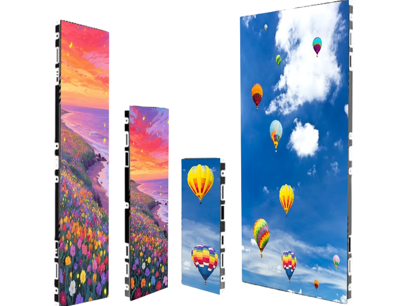
.jpg "China Indoor Stage LED Video Wall Manufacturers, Rental Panels, High Refresh")
.jpg "Can You Buy From DIY LED Display Manufacturers?")